Course Info
Class: MWF 3:35-4:25pm (09/02/2008 - 12/10/2008), Room MechE 212.
Course web page: http://www.ece.umn.edu/users/kia/Courses/EE5323
UNITE page: https://hermes.unite.umn.edu/index.html (opens in a new tab)
WebVista page: http://myu.umn.edu > My Courses tab>WebVista C under EE5323>Login (opens in a new window). Note from Web vista C on setting up your browser, etc.
Class mailing list: subscribe here ( If you choose to receive the daily digest, then you will not receive individual messages as they are posted: instead they will be aggregated into a single message and sent to you at the end of the day).
Cadence tutorial pages: Cadence tutorial pages.
Midterm exam: Mon Oct 20, in class, open book, open notes.
Final exam: 1:30-3:30, Thu 12/18/08, open book, open notes.
Catalog Description:
Combinational static CMOS circuits. Transmission gate networks. Clocking strategies, sequential circuits. CMOS process flows, design rules, structured layout techniques. Dynamic circuits, including Domino CMOS and DCVS. Performance analysis, design optimization, device sizing.
Course Objectives:
This class is intended to be an introduction to the design of digital Very Large Scale Integrated (VLSI) circuits. It is the first part of a two-semester sequence: this part focuses on the transistor-level and logic-level aspects, while the second part, EE 5324, concentrates on more advanced issues in design (e.g., supply nets and clocks, controlling power, memory design, etc.). The main objective of the two-semester sequence is to provide the student with the capability of designing digital VLSI circuits. The term-long project involves heavy use of Cadence schematic and layout tools which are the de-facto design software in the semiconductor industry.
Prerequisites:
The prerequisites to this class are EE2301 (a first class on digital design) and EE3115 (a first class on analog and digital electronics), or equivalent. Students are expected to have a working knowledge of digital logic design and basic CMOS circuits.
Text:
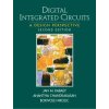
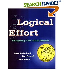
[Rab02] is required. Both books are on reserve in Walter Library at the basement circulation desk
*Note: book cover images from amazon.com.
Administrative
Please check the "Announcements" link regularly.
Grading:
- 20% Homework and quizzes - no late homework, no copying!
- 20% final project (two phases)
- 25% Midterm - open note.
- 35% Final exam
Policies:
- Cheating of any kind is extremely serious and may result in a course grade of F and/or expulsion from the University. Refer to http://www1.umn.edu/oscai/ for the definition of academic integrity and a FAQ on scholastic dishonesty.
- Homework submissions are due before class starts (or in instructor's mailbox 5 minutes before class). You have a total of 3 days of grace period that can be used for late homework. You could use it all on one assignment, or say, 12 hours each on 6 homework submissions. After the grace period is over, no late homework will be graded.
- Collaboration on homework problems OK, copying not OK.
- Include your student ID number on all homework assignments and exams.
- No extra work will be accepted for improving the final grade
- University senate statement on the 'I' grades:
"The I shall be assigned at the discretion of the instructor when, due to extraordinary circumstances, the student was prevented from completing the work of the course on time. The assignment of an I requires a written agreement between the instructor and student specifying the time and manner in which the student will complete the course requirements. In no event may any such written agreement allow a period of longer than one year to complete the course requirements." The 'extraordinary circumstances' must be verifiable. - Makeup exams will only be allowed for situations similar to ones requiring an 'I' grade. Again, the extraordinary circumstances requiring a makeup exam must be verifiable.
- I recommend that you read documents on The Student Conflict Resolution Center web page.
Personnel:
Kia Bazargan (Instructor)
| Email: | [email protected] |
| Phone: | (612) 625-4588 |
| Office: | EE/CSci 4-159 |
| Office hours: | Mon 10-11 Fri 2-3 |
Satish Sivaswamy (Teaching Assitant)
| Email: | [email protected] |
| Office: | VLSI Lab EE/CSci 1-200 |
| Office hours: | TTh 11-12 |
Course Outline
- CMOS device physics and models
- INVERTER gate
- Basic channel equations
- Design process: schematic, layout, simulation
- INVERTER gate
- Basics of CMOS circuits: basic gates, combinational and sequential logic
- Essentials of semiconductor processing
- CMOS layout design
- Delay calculation and optimization; logical effort
- Designing wires
- Dynamic styles: domino and pass transistor logic
- CMOS Design
- Adders
- Basic adders: carry propagation, Manchester Carry Chains
- More complex adders: Carry Look-ahead, Carry Save Adder, Brent-Kung
- Fast adders: Carry-Select adder, Wallace tree
- Multipliers
- Shift/Add multiplication
- Booth encoding
- Multiplication by constants
- Floating point multiplication
- Division / Square root
- Shift/rotate operations
- Adders

